Question: is the 555 complete in the Boolean sense? That is, can any Boolean function be realized as a network of 555 chips?
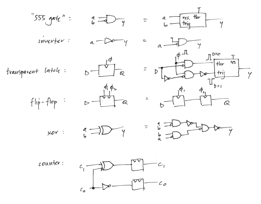
Answer: yes. Tie the threshold pin high---this essentially disables the 555's internal latch. Now provide inputs to the reset and trigger pins and take the output from either the totem-pole output or the open-collector output with a suitable external load. Here is the truth table:
| reset | trigger | output |
|---|---|---|
| 0 | 0 | 0 |
| 0 | 1 | 0 |
| 1 | 0 | 1 |
| 1 | 1 | 0 |
This is a somewhat unusual gate---it can be interpreted as the negation of the conditional operator, or as an AND gate with one of the inputs inverted. But it is complete: an inverter can be obtained by tying reset high; now using this inverter, invert the reset input and one has a NOR gate made from two 555s; the NOR gate is known to be complete. Of course a given Boolean function will be implemented most efficiently by telling the logic synthesis tool (or human designer) to map directly onto the "555 gate" rather than use the NOR-gate construction; but the NOR is a convenient route to the completeness proof.
Storage elements can be made from cross-coupled gates or, as we will see below, from 555s configured to use their internal latch, which is slightly more efficient.
So we immediately have the whole of digital design available to us. One can imagine various projects---counters, state machines, memories, computers---all of which can be built from a large pile of 555s. Of course the same could be said about a large pile of 7400 TTL NAND gates, or transistors. What sorts of constructions, then, should we pursue that would be most interesting from a 555-chip point of view?
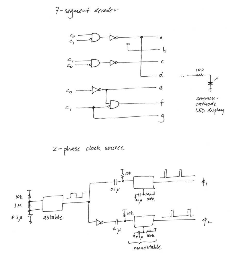
It's just my opinion, but it seems best to try to use as much of the 555 internal structure as possible to implement gates and latches efficiently. For combinational logic, we have the raw "555 gate" and the possibility of using a wired-AND connection with the open-collector/open-drain output and a resistor pullup (at the cost of some static power; "NMOS"). For sequential logic, we need to choose a storage element and a clocking scheme. Below is one such choice together with an example circuit: a 2-bit counter and a 7-segment decoder, enough to serve as a proof of principle.
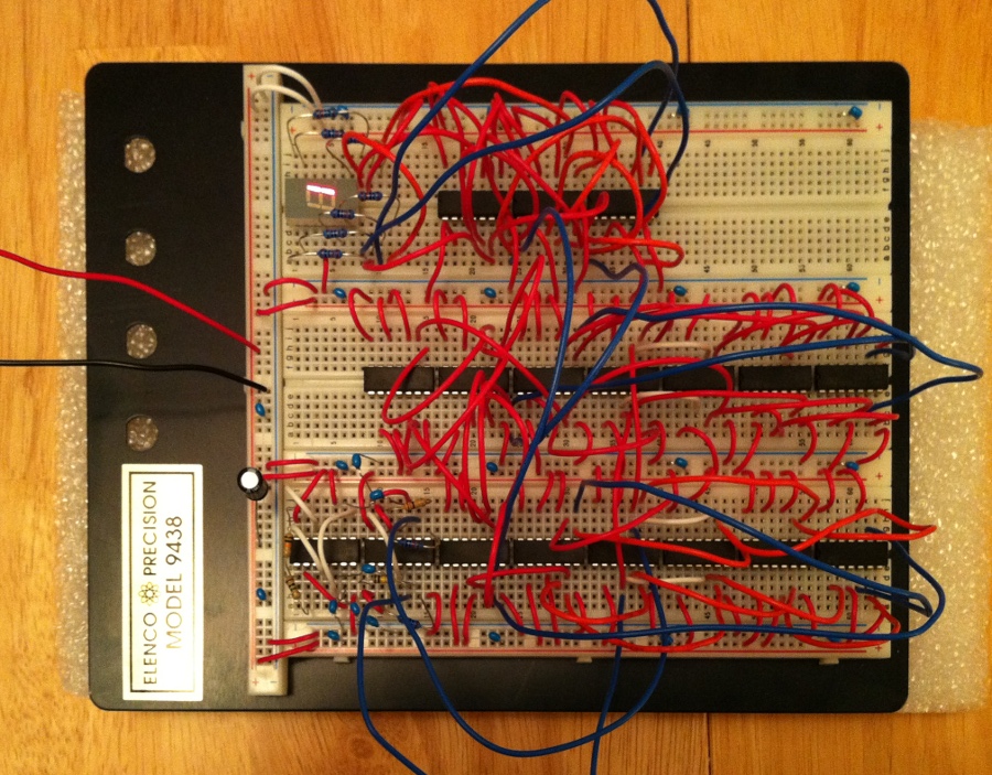
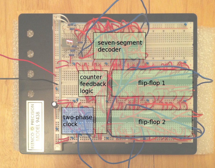
Here is the breadboarded system, together with an annotated picture showing the location of functional blocks. There are a total of 18 556 packages, equivalent to 36 555s.
Video of the system with the clock set to about 2 Hz:
Why two-phase clocking rather than edge-triggered logic in the modern style? Well, edge-triggered flip-flops are somewhat trickier to design and verify. A two-phase clock feeding a pair of transparent latches is almost bulletproof. One has complete control over the duration of non-overlap between the two phases (to control skew) as well as the overall frequency of the clock. Even clock glitches can be tolerated (provided there is no crosstalk between the phases), since a single clock phase is idempotent.
This logic technology should have no trouble scaling up to larger systems. I had hoped to do this small 4-bit CPU:
//
// tiny Harvard-architecture 4-bit CPU
//
// February 2011
// Peter Monta
//

module cpu(
  input clk, reset,
  output reg [4:0] pc,       // program counter
  input [7:0] ir,            // instruction
  output [3:0] addr,         // data address
  input [3:0] din,           // data input
  output [3:0] dout,         // data output
  output wr                  // write signal
);

  reg [3:0] a;         // accumulator
  reg c;               // carry flag

  assign addr = ir[3:0];
  assign dout = a;
  assign wr = ir[7:5]==3'b001;

  wire [3:0] b = ir[4] ? ir[3:0] : din;       // data memory or literal
  wire z = a==4'd0;                           // zero flag

  always @(posedge clk)
    if (reset)
      pc = 0;
    else begin
      pc = pc+1;
      case (ir[7:5])
        3'b000: a = b;                     // lda
        3'b001: ;                          // sta
        3'b010: {c,a} = a + b + c;         // adc
        3'b011: a = ~(a|b);                // nor
        3'b100: pc = ir[4:0];              // jmp
        3'b101: if (!c) pc = ir[4:0];      // jnc
        3'b110: if (!z) pc = ir[4:0];      // jnz
        3'b111: c = ir[0];                 // setc
      endcase
    end

endmodule
but there just wasn't time. Its size (after doing the synthesis manually) is 387 555-chips, or 194 packages using the 556. That would need a PCB; it's too big to wire by hand. Here's a PDF of the schematic and the kicad source files.
Possible future directions: